We want to optimize the parts of the datacenter hardware such that the cost of operating the datacenter as a whole would be lower, we need to think about it as a whole.
Datacenter CPUs
Desktop CPU vs Cloud CPU
- Isolation:
- Desktop CPUs have low isolation, they are used by a single user.
- Cloud CPUs have high isolation, they are shared among different users.
- Workload and performance: usually high workloads and moving a lot of data around.
They have a spectrum of low and high end cores, so that if you have high parallelism you can use lower cores, while for resource intensive tasks, its better to have high end cores, especially for latency critical tasks.
Datacenters have developed own chips for custom software too. This is ok to specialize on their own workloads and get better on that market.
Also NVIDIA is designing a CPU, so that they can couple them together and co-optimize it (increases 30x memory movement, Grace Hopper architecture CPU linked with GPU). Alps cluster at ETH have 10k of those GPUs.
These are some examples of CPUs designed lately:
- AWS Graviton Arm CPU
- Microsoft Cobalt Arm CPU
- Google Axion Arm CPU
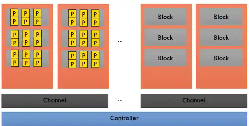
Two socket datacenter server
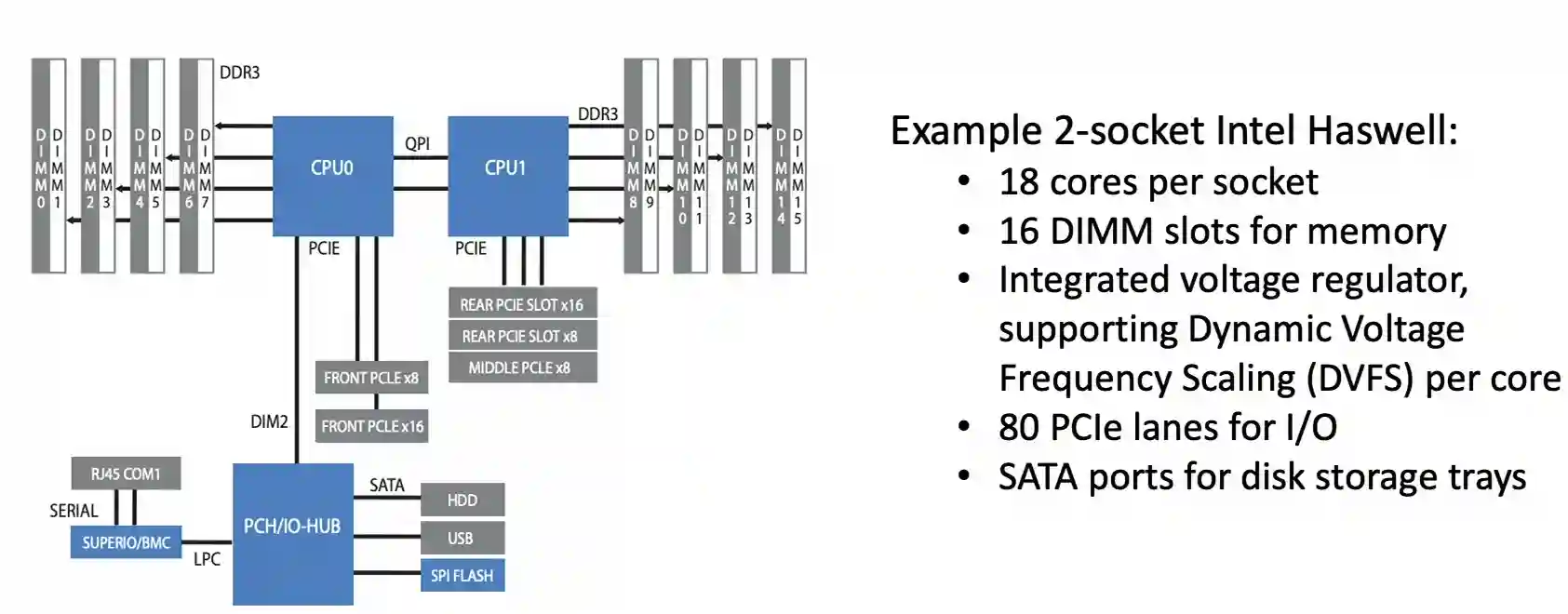 These are some of the design considerations that one need to take into account to design a chip more specific for cloud environments:
- Type of core: “brawny” or “wimpy”
- Meaning better more energy hungry but more efficient cores, or less energy hungry but less efficient cores, but in more quantity?
- Number of cores
- Number of sockets and NUMA topology
- Cache hierarchy and size
- Isolation mechanisms for multi-tenancy (for performance & security)
- Integration with hardware accelerators, network devices, etc.
- Power management.
Usually these cores are brawny (performance) cores. Nowadays cores have dynamic voltage frequency scaling that allows frequency scaling per core.
NUMA Technology
NUMA stands for Non-Uniform Memory Access. It's a memory design used in multi-socket and some multi-core systems where each CPU (or group of cores) has its own local memory and shared access to remote memory.
In simpler terms: Not all memory in the system is equally fast to access from every CPU core.
The above image on two core datacenter server is an example of a NUMA architecture, where each socket has its own memory and can access the other socket memory with a higher latency.
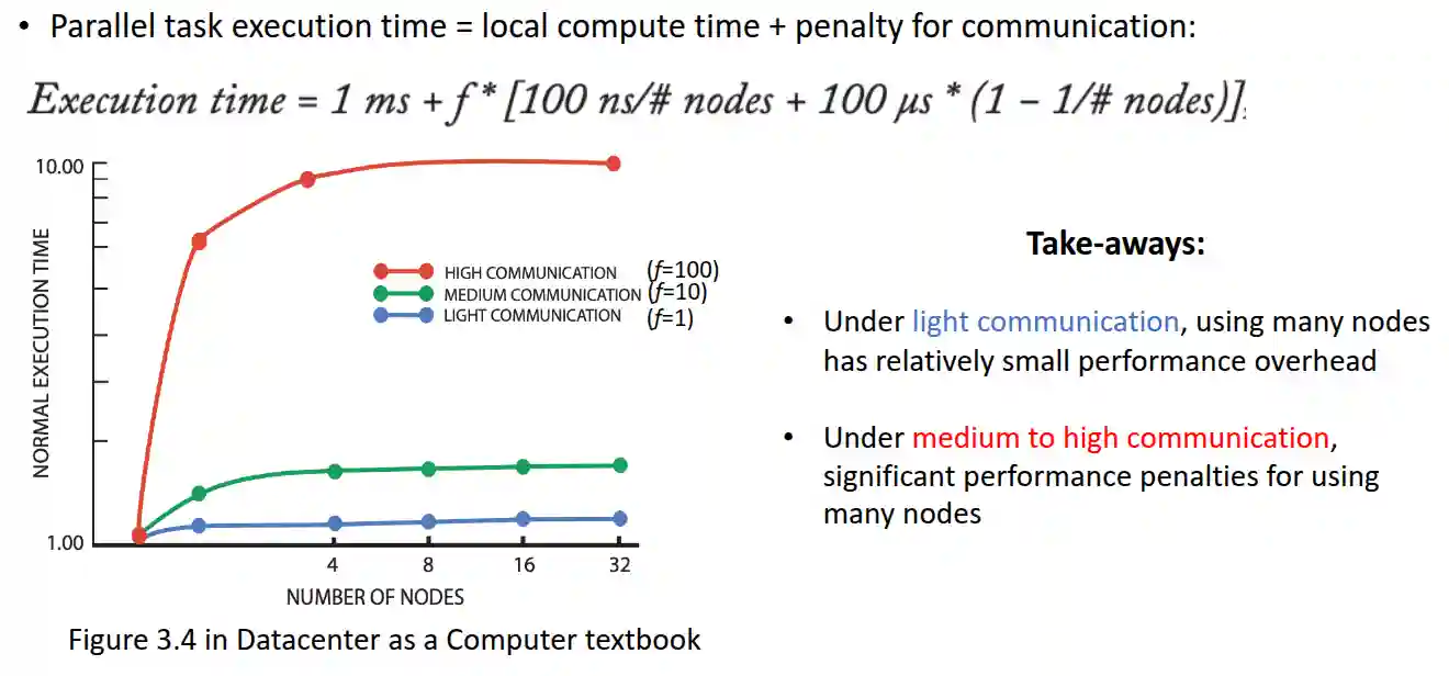
Performance with Cluster size and Communication
The number of cores to allocate to a single application should depend on the type of application that is running, more communications means bigger overheads.
The basic takeaway is that you can optimize well if the program does not need to communicate a lot, and sometimes it is huge, the two socket architecture is considered the sweet spot for both performance and cost.
Amdahl's Law
This law defines the speed up that you can achieve after you parallelize the code. Usually it is defined as:
Where is the parallelizable part of the code, and is the number of processors.
Gustafson's Law
Problem size scales with number of processors (constant work per processor). This means: as we add more processors in the system, the compute needed to solve the same problem is more, we can see this as the reverse side of the Amdahl's law, since perhaps some compute is for communication. But it is more intended about solving larger problems at the same time.
Intel Cache allocation technology
Instead of every core/application having free rein over the full L3 cache, CAT lets you assign specific portions of that cache to specific workloads.
This is the main, idea, in this manner we don't have many conflict evictions due to this part.
- Enables partitioning the ways of a highly-associative last-level caching into several subsets with smaller associativity.
- Cores assigned to one subset can only allocate cache lines in their subset on refills, but are allowed to hit in any part of the last-level cache (LLC).
- It is usually implemented using bitmasks on the associativity of the cache, see Cache Optimization. This enables higher priority applications running on some LLC to get more cache size for allocation during runtime.
Real-time systems or latency-sensitive apps (like video streaming, trading, or telco) can't tolerate unpredictable cache behavior.
Other technologies like Dynamic Voltage Frequency Scaling (DVFS) enables core-independent scaling. And there is no bandwidth isolation.
CPU Types and Power Management
As we saw when studying the assignment related to Skylake Microprocessor, there are efficient and perfromance cores, in this context called wimpy and brawny cores. The former is more energy efficient (2x) but much slower 5x, while the latter is faster, yet because of Ahmdal's law, it has much performance variability.
There are p-states and c-states:
- p-states: power consumption when the system is executing code
- c-states: power consumption levels when the system is idle.
Different cores have different consumption, we can control the performance by controlling frequency and power.
Towards Hardware specialization
- CPU have low latency but also low memory throughput, and they are general purpose (instruction fetching, data fetching, execution storage etc.)
- GPU have high latency but high memory throughput, good for memory-bound computations.
- These GPUs have a high overhead in moving data, so when you have computations where you need to access data that is not sequential in memory, it is probably difficult to have a benefit from them.
- The case above is not true for ML workloads, where the main bottleneck was the memory for the matrix multiplications, see Cache Optimization.
- Google has been developing his own GPU, called TPU, they predicted high workload for inference, and wanted to be less dependent from hardware companies.
- The specialization trend is for everything (NIC, memory, storage, networking, more and more processors are seen to be developed in the next years), there are lots of money flowing to unique accelerators. Currently a server lasts about 6 years in a datacenter (average lifetime) (meeting performance requirements and hardware reliability).
Other examples are NVIDIA GB300 NVL72, or Project Ceiba from Microsoft, which is a custom chip for AI workloads, they are trying to go more for scale up now instead of scale out.
Compute Express Link
CXL is an open standard cache-coherent interconnect for processors, memory expansion, and accelerators. It introduces a new level in the memory hierarchy.
- Maintains coherency between CPU memory and memory on attached devices.
- Enables resource sharing (or pooling) for higher performance, reduces software stack complexity, and lowers overall system cost. Why is it needed?
- Modern workloads have high memory capacity requirements. Spilling to SSD is too slow. Thus, need to make remote memory access fast!
- Accelerators are increasingly common and have their own memory need high-bandwidth access between CPU and devices, this is why a new protocol is needed.
See Compute Express Link for other info about this section.
FPGAs
For example the TCP stack is using lots of cycles, you could program a chip just optimized for these kinds of operations, FPGAs are good with those specialized kinds of computations where neither CPU and GPUs are good at:
- Network operations
- Data parallelism with irregular accesses.
- Operations that are not float or int operations (filtering packets in network settings for example).
- Encryption operations Basically everything that could benefit offloading computation to other parts, when the CPU is still busy, but putting a GPU or TPU would be overkill.
The tooling here in the chip design takes a lot of time. One example of a technology that uses FPGAs in a similar manner is AQUA, pushing computational resources for reduction and aggregation closer to the data (reducing network traffic), layer on top of S3 for Redshift.

Image from course slides CCA 2025 ETHz | FPGA can be used to offload many common tasks from CPUs, (e.g. network encryption, serialization and similars), this makes the NIC quite faster, using custom smartNIC based on FPGA, see [[@firestoneAzureAcceleratedNetworking2018
We show that FPGAs are the best current platform for offloading our networking stack as ASICs do not provide sufficient programmability, and embedded CPU cores do not provide scalable performance, especially on single network flows.
Datacenter Structure
The whole datacenter is designed to minimize the ownership cost of the system. This section is anyways mostly just introductory.
Electrical Systems
To be done.
Cooling Systems
Heating is a huge issue inside datacenter systems. We have many many systems up to handle a good cooling behaviour within the systems.

some example of how datacenters are organized to favor better cooling
Analyzing Bottlenecks
Profiling a warehouse scale computer
These are mainly results from the paper (Kanev et al. 2015).
we show significant diversity in workload behavior with no single “silver-bullet” application to optimize for and with no major intra-application hotspots.
One main observation is that the workloads are diverse, and you cannot just optimize for a single kind of workload. They basically assert that there is not single bottleneck for performance of the Warehouse scale computer.
- Top 50 binaries cover only 60% of the total execution time, also in modern AI jobs, the statistics should be similar.
The data-center tax
There is a data-center tax associated with moving things around. and communication.

Image from [[@kanevProfilingWarehousescaleComputer2015
Types of stalls
We define three types of values:
- Retiring is considering useful work, the rest are sources of overhead.
- Front-end stall: captures all overheads associated with fetching & decoding instructions
- The instruction set needed is 100x the L1 instruction cache (and this is growing 20% a year), but it is impractical to grow the cache size so much.
- We can try to prefetch the part of the data that matters in the L1 cache, but not sure how is this possible. -> What AsmDB does, when it recognizes common instruction sequences.
- Introduce custom instructions + 5% better instructions per cycle.
- Back-end stall: captures overheads due to data cache hierarchy and lack of instruction-level parallelism (see Skylake Microprocessor for more information about this parallelism).
Most of the overhead are from back-end stalls.
AsmDB
From the paper (Ayers et al. 2019), collects data about block-level instruction usage into an assembly database, so that:
- You know what instructions are used, so perhaps you can manually optimize for it.
- benchmarks for better compilers in i-cache design (software prefetch instructions).
- Data source for compiler driven improvements of the binaries. Gets 5% better instruction per cycle, saving millions of dollars.
Imbalanced resource usages
The resource usage in the datacenter are basically independent with each other, it is quite hard to predict a precise ration between CPU and memory that is needed to optimize the resources for a specific data center. By disaggregating resources, we are able to scale them independently.

Idea of a solution: Dynamically allocate the ratio of resources an application needs by using compute & storage components connected over a network
There is something similar of storing Graph Databases in disaggregated manners in the disk, but in a wholly different field.
The Storage Hierarchy
We need to expand the classical single server memory architecture (see Memoria) to datacenter level. Now we have rack memory and datacenter memory, and the idea that higher latency with higher memory possibility is still valid here.
Introduction to Memory Types
Access Speeds
Usually now the bottleneck is the network. One observation is that the remote latency of the disk is similar to the local disk latency (disk seek is the bottleneck, wire transfer is faster). One interesting observation is that rack memory and cluster memory seeks are faster than local disks and they also have higher bandwidth!
| Configuration | Component | Capacity | Latency | Speed |
|---|---|---|---|---|
| ONE SERVER | DRAM | 256GB | 100ns | 150GB/s |
| ONE SERVER | DISK | 80TB | 10ms | 800MB/s |
| ONE SERVER | FLASH | 4TB | 100us | 3GB/s |
| LOCAL RACK (40 SERVERS) | DRAM | 10TB | 20us | 5GB/s |
| LOCAL RACK (40 SERVERS) | DISK | 3.2PB | 10ms | 5GB/s |
| LOCAL RACK (40 SERVERS) | FLASH | 160TB | 120us | 5GB/s |
| CLUSTER (125 RACKS) | DRAM | 1.28PB | 50us | 1.2GB/s |
| CLUSTER (125 RACKS) | DISK | 400PB | 10ms | 1.2GB/s |
| CLUSTER (125 RACKS) | FLASH | 20PB | 150us | 1.2GB/s |
From Jeff Dean Tables:
| Operation | Time |
|---|---|
| L1 cache reference | 1.5 ns |
| L2 cache reference | 5 ns |
| Branch misprediction | 6 ns |
| Uncontended mutex lock/unlock | 20 ns |
| L3 cache reference | 25 ns |
| Main memory reference | 100 ns |
| Decompress 1 KB with Snappy [Sna] | 500 ns |
| "Far memory"/Fast NVM reference | 1,000 ns (1 us) |
| Compress 1 KB with Snappy [Sna] | 2,000 ns (2 us) |
| Read 1 MB sequentially from memory | 12,000 ns (12 us) |
| SSD Random Read | 100,000 ns (100 us) |
| Read 1 MB bytes sequentially from SSD | 500,000 ns (500 us) |
| Read 1 MB sequentially from 10Gbps network | 1,000,000 ns (1 ms) |
| Read 1 MB sequentially from disk | 10,000,000 ns (10 ms) |
| Disk seek | 10,000,000 ns (10 ms) |
| Send packet California->Netherlands->California | 150,000,000 ns (150 ms) |
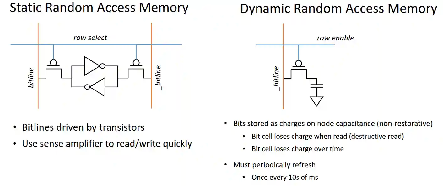
Types of Memories
- SRAM: Static RAM, used for cache. Fast and expensive (cost per bit).
- We need six transistors for a SRAM
- Amplifier to read quickly.
- No worries about refreshes.
- DRAM: Dynamic RAM, used for main memory. Slower and cheaper.
- Stores one bit with one transistor (a special one)
- Much higher density compared to SRAM
- Flash storage: Used for SSDs. Slower than DRAM but faster than traditional HDDs.
Rough comparisons for DRAM : Flash : Disk
- Cost per bit: 100 : 10 : 1
- Access latency: 1 : 5,000 : 1,000,000
DRAM: Memory-Access Protocol
As we studied in Circuiti Sequenziali when developing a small memory, we need a system to index into the memory and retrieve its content. This is done by a memory controller, which implements the memory-access protocol with its row decoders and similars.
DRAM Operations
DRAM has an access protocol that allows for some commands:
- ACTIVATE (open a row)
- It opens the whole row and loads content into row buffer, after a nanosecond delay (called Row to Column Delay)
- Usually one row is 4k to 32k of data, DDR4 has 8K rows each with 8KB
- READ (read a column)
- It reads the specific Column, but needs to destroy that data after some amplification, the data needs to be restored.
- The number of banks is around 16 to 32. per chip, and you usually have 8 to 16 DRAM chips, so you can read about 4 megabyte just in one cycle if its always in the banks.
- WRITE
- WRITING trashes the row buffer temporarily and forces a restore cycle later.
- PRECHARGE (close row)
- Resets the bank to a neutral state so that another row can be read.
- REFRESH
- Every 64ms you need a refresh to maintain the memory, when a refresh is occurring the DRAM cannot do other things.
Row policies
And we also have row policies (open rows use energy), and you can also optimize for the row opening prediction. (open-row policy, and closed-row policy), or you can also use speculative row access policies.
Open Row:
- Keep the row open until it is needed for another, only then you can precharge
- This saves latency if you know that row will be used many times.
Closed Row
- Close the row as soon as you are done with it, unless there is some request that is already going for that row.
- Helps to avoid conflict for changing rows.
Speculative version Attempt to predict whether you need to close or open that row.
Flash Storage
This looks like a good introductory source.
This is for non-volatile memory, SSDs. They use specific transistors to control the charge on the gates and then understand if it is one or zero. Lower charge means 1. You can use different levels to directly encode 2 bits instead of one.
- Charge modulates the threshold voltage of the underlying transistor
- You can also store more than one bit in one transistor, this is the multi-level cell.
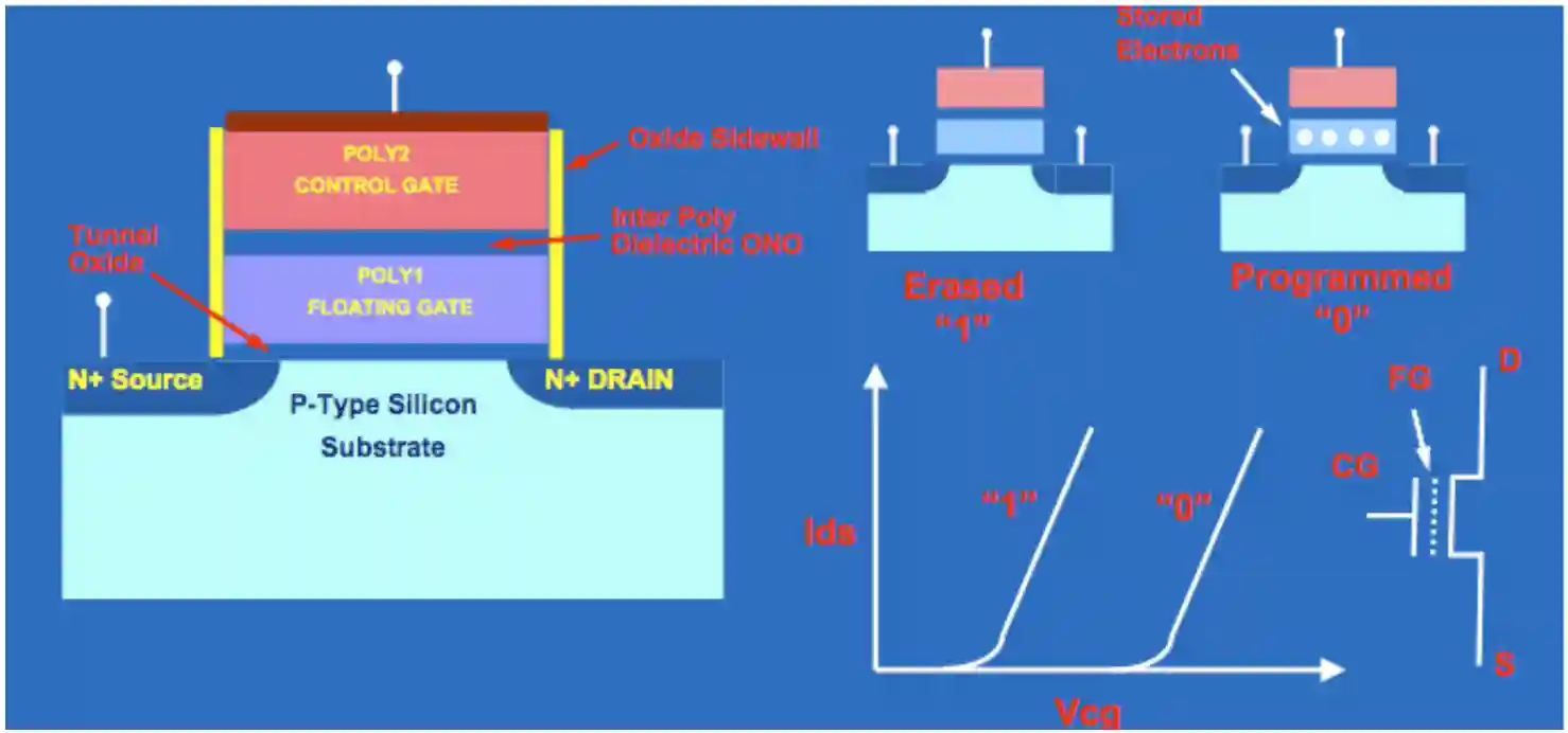
Working Principles
Floating-Gate Transistor: At the heart of a flash memory cell is a MOSFET (Metal-Oxide-Semiconductor Field-Effect Transistor) with the following structure:
- Control Gate (CG): This gate is used to control the flow of current through the transistor's channel, similar to a regular MOSFET.
- Floating Gate (FG): This gate is electrically isolated by an insulating layer (typically silicon dioxide) surrounding it. The floating gate's charge determines the threshold voltage of the transistor, which in turn dictates whether the cell represents a binary '0' or '1'.
Data Storage Mechanism:
- Writing (Programming): To store data, a voltage is applied to the control gate. This causes electrons to tunnel through the insulating layer and become trapped on the floating gate. The presence of these electrons increases the threshold voltage of the transistor. This state typically represents a binary '0'.
- Reading: When reading data, a voltage is applied to the control gate. The current flow through the transistor's channel is then sensed. If the threshold voltage is low (no or few electrons on the floating gate), current flows, representing a binary '1'. If the threshold voltage is high (electrons on the floating gate), current does not flow, representing a binary '0'.
- Erasing: To erase data, a higher voltage of the opposite polarity is applied, typically to the source terminal. This forces the trapped electrons off the floating gate through quantum tunneling, returning the cell to its original, unprogrammed state (representing a binary '1'). In NAND flash, erasure typically happens in larger blocks of cells, while NOR flash allows for block or chip erasure
Flash Storage Types
- SLC single-level cell
- Faster but less dense
- More reliable (100K -1M erase cycles)
- ~$1.5/GB
- Used in “enterprise” drives (i.e. Intel Extreme SSDs)
- Good for write intensive workflows.
- MLC: multi-level cell
- Slower but denser
- Less reliable (1K - 10K erase cycles, becomes a problem with write intensive workloads)
- $0.08/GB (two orders of magnitude cheaper!)
- Used in consumer drives (thumb drives, cheap SSDs, etc.)
- eMLC for enterprise use designed for lower error rates
Internal Architecture of Flash Storage
Flash storages have controllers, connected to blocks of data, these blocks (blocks contain pages) need to be erased at the same time, while pages are the minimum unit of read/write. Usually we have:
- 512bytes or 8kb per page
- 64-256 pages per block
- About 1 to 16 chips, capacity of 1 to 16. you see that one block holds about 512MB to 2GB.
Flash Operations
- Read the contents of a page
- 20-80us (reading operation is much much faster!)
- One problem is that each chip can process one operation per unit time.
- This creates sorts of interference (quite big interference!).
- Write (program) data to a page
- Only 1-0 transitions are allowed
- Writing within a block must be ordered by page
- 1-2ms
- Erase all bits in a block to 1
- Pages must be erased before they can be written
- Update-in-place is not possible
- 3-7ms
Because of physical constraints, just because of the physical constraints of these devices. There could be access interferences that need to be handled well. There is a big possibility in intereference because of this part.
Write amplification
Write amplification is the ratio of physical pages written to Flash for every logical page written by the user application. This ratio is greater than 1 because the Flash Translation Layer performs additional writes to erase blocks without losing valid data.
Reliability of Flash Storage
In this section we list some of the reliability issues that can happen with flash storage.
- Wear out
- Flash cells are physically damaged programming and erasing them
- Writing Interferences
- Programming pages can corrupt the values of other pages in the block
- Read Interferences
- Reading data can corrupt the data in the block
- It takes many reads to see this effect
Flash Translation Layer
How can you handle some pages that just work out? We would like to have an interface that is closer to the original disk based access, this is what the FTL (flash translation layer) does.
The FTL keeps a datastructure for a map (address to physical page address) and information for each block (e.g. page counts) to know when to remove blocks. Writes are over a write pointer.
- Read memory: Tells you where to read for block and lines given a memory access.
- Write memory: Chooses where to write based on a write pointer, then you invalidate the old block.
- Count valid blocks
- Decrease available blocks count.
- If the a page has zero good pages, then it is just deleted with that hardware operation and then can be reused.
- When we want to erase, we need to move the good blocks to another part and only then erase it.
Structures in the FTL
You have two datastructures:
- Map: maps device addresses to actual physical addresses in the Flash Storage.
- Block Info Table: this keeps information about every blocks: valid pages, erase count (too see if the block is still in working condition (it has a flag for this)), and a sequence number.
After a write, it there was something already there, you just invalidate the block (don't erase it yet, since we would need to erase the entire block), and write to a different page in a different block. When you need to erase, you move every valid block, and set the block state to erased.
Datacenter Networking
Each server has a NIC (Network Interface Card) that connects to a switch, which connects to other switches and servers.
Desiderata of Networking
- Low latency
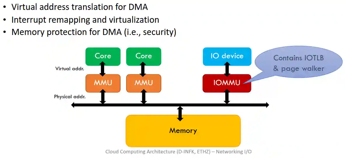
- Security through virtualization, see Container Virtualization, and IO memory virtualization, see Virtual Machines.
- We need IO Memory Management Units to virtualize DMA accesses.
- IOMMU unit that intercepts DMA for virtualization, and translated it into physical addresses for IO parts.
SR-IOV
Single Root I/O Virtualization (SR-IOV) allows a specification for sharing a PCIe device to appear as multiple guests. This enables more efficient sharing of network resources among virtual machines (VMs) or containers.
- Allows a single device on a single physical port to appear as multiple, separate physical devices
- Hypervisor is not involved in data transfers à set up independent memory space, interrupts and DMA streams for guests
- Requires hardware support
- i.e., the I/O device must be SR-IOV capable We have explored this part in Virtual Machines.

PF stands for private function, which is the privileged hardware function for accessing the network interface, while VF is the virtual functione exposed to the virtual machine, who then uses to access directly the hardware in a secure manner. | image from [[@firestoneAzureAcceleratedNetworking2018
IO Memory Management Unit
Communicating data availability
Two main ways, interrupting and polling. We have presented these two methods in Note sull'architettura.
Polling is not a bad approach within a datacenter setting (not much context switching for interrupts), that is still ok.
Slow networking software
Linux kernel is very slow in handling network part, it has been designed to be general, and offers sometimes too many generalizations that often hinder the latency aspect. The throughput for HW limits is much much higher. This is a strong motivator to write the best possible software for that specific hardware.
For example take the TCP/IP networking (Classical, see Livello di Rete) Sources of overhead in packet processing
- Interrupts & OS scheduling
- Kernel crossings (context switches)
- Buffer copies
- Packetizing & checking for errors
- Memory latency
- Poor locality of I/O data processing
- Memory bandwidth not an issue, why? Example
- 64 byte Ethernet packets @ 10Gbps
- This is 20M packets/sec
- Naively done: 20M interrupts/sec, which is a huge overhead!
There are some ideas on how to optimize the slow networking software:
- Move everything to user space and optimize the software
- Offload processing to NIC hardware, as (Firestone et al. 2018) does.
NIC optimizations
- Checksum Offload:
- NIC checks TCP and IP checksum with special hardware (CRC).
- Large Segment Offloading (LSO) (at transmit):
- NIC breaks up large TCP segments into smaller packets.
- Automatic Header Generation:
- Large Receive Offload (LRO):
- Combines several incoming packets into one much larger packet for processing.
- Header Splitting (at receive):
- NIC places header & payload in separate system buffers.
- Improves locality: (Why?)
- Allows more prefetching & zero copy.
- Interrupt Coalescing: so that you don't need so many interrupts to handle single packets, but you can process in batches.
- It is also possible to use steering based optimizations.
References
[1] Kanev et al. “Profiling a Warehouse-Scale Computer” ACM 2015
[2] Ayers et al. “AsmDB: Understanding and Mitigating Front-End Stalls in Warehouse-Scale Computers” ACM 2019
[3] Firestone et al. “Azure Accelerated Networking: SmartNICs in the Public Cloud” 5th USENIX Symposium on Networked Systems Design and Implementation 2018